Tic Tac Toe on FPGA
Tic-tac-toe originated from the ancient Roman Empire around the first century BCE, and it was called Terni Lapilli. The rules of the game differ as each player only had three pieces, moving around the empty spaces to keep playing. The first print reference of the game appears in Britain with the name “Noughts and Crosses” in 1864. The name “tic-tac-toe” was renamed from “Noughts and Crosses” in the 20th century in the USA and is the earliest known game to display visuals on a video monitor. Although Tic-tac-toe appears simplistic to play, it contains 138 terminal board positions and 255,168 possible ways these terminal board positions is obtained.
- The game is played on a grid that’s 3 squares by 3 squares.
- You are X, your friend (or the computer in this case) is O. Players take turns putting their marks in empty squares.
- The first player to get 3 of her marks in a row (up, down, across, or diagonally) is the winner.
- When all 9 squares are full, the game is over. If no player has 3 marks in a row, the game ends in a tie.
Overview
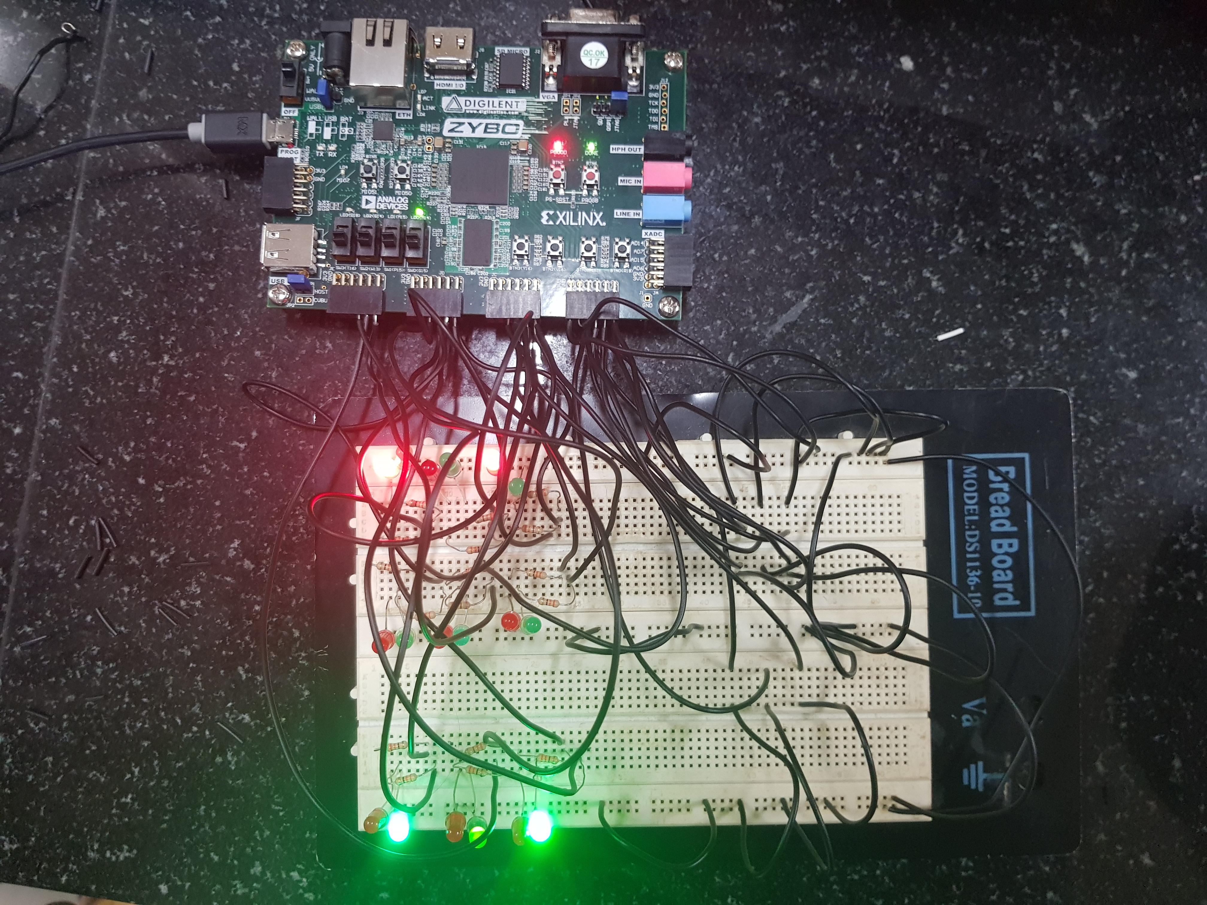
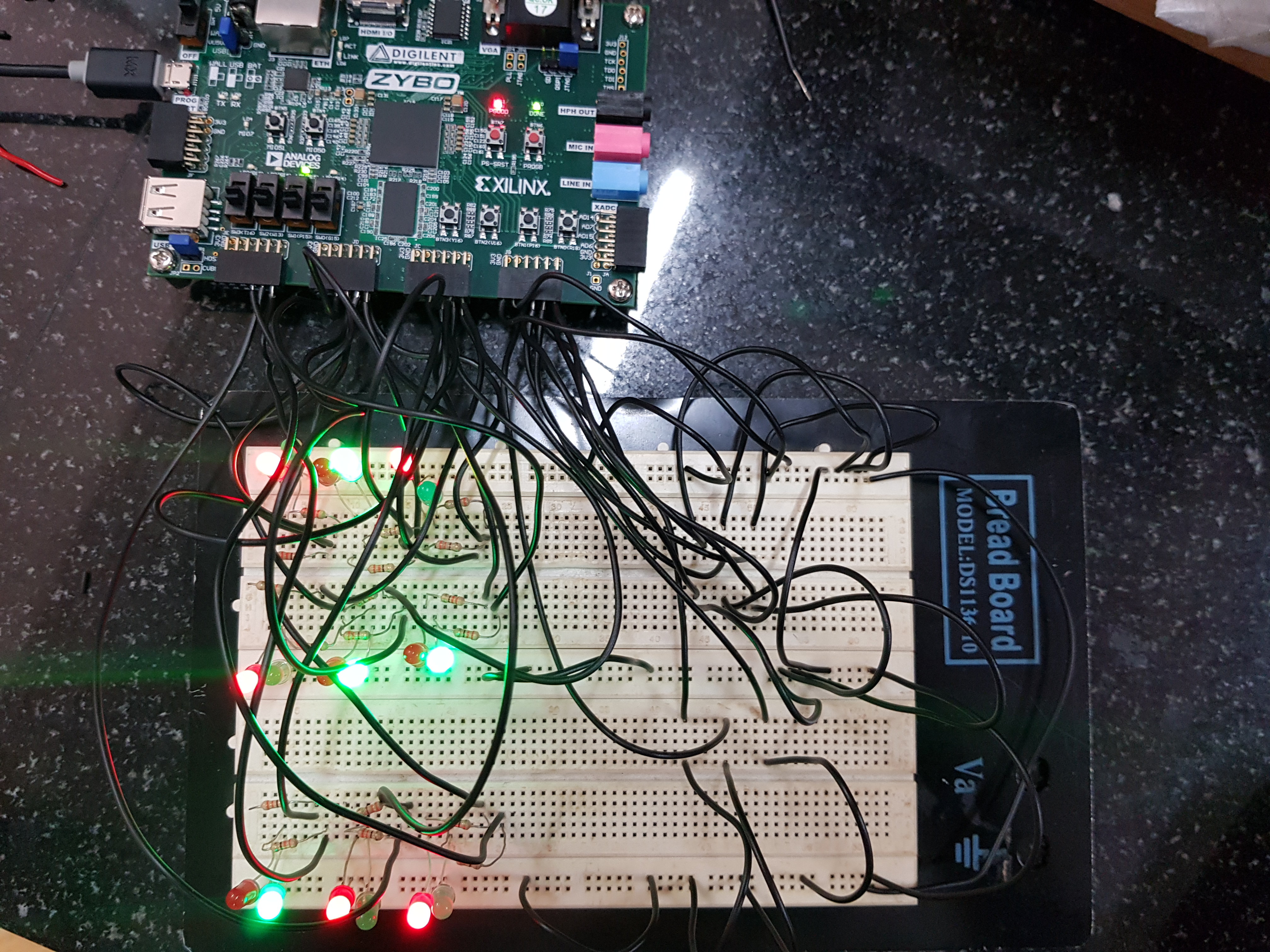
TIC-TAC-TOE game is programmed in ZYBO Board via Verilog. The game consists of 9 push buttons in the form of a 3 x 3 grid, corresponding to the inputs of the user. It also consists of a 3x3 LED matrix with each cell consisting of a RED LED and a GREEN LED where RED corresponds to X and GREEN corresponds to Y. There are 3 LEDs to indicate a win, draw, and illegal move. The players take turns alternatively. On each turn when the player pushes a button corresponding LEDs start to glow at the respective grid location. Based on the player’s status the corresponding indicator LED will glow.
Materials
- FPGA - ZYBO
- Bread Board
- 9 x Red LEDs and Green LEDs
- Jumper Wires
- 9 x Push Button
- 18 x Resistors (330 Ω)
Theory
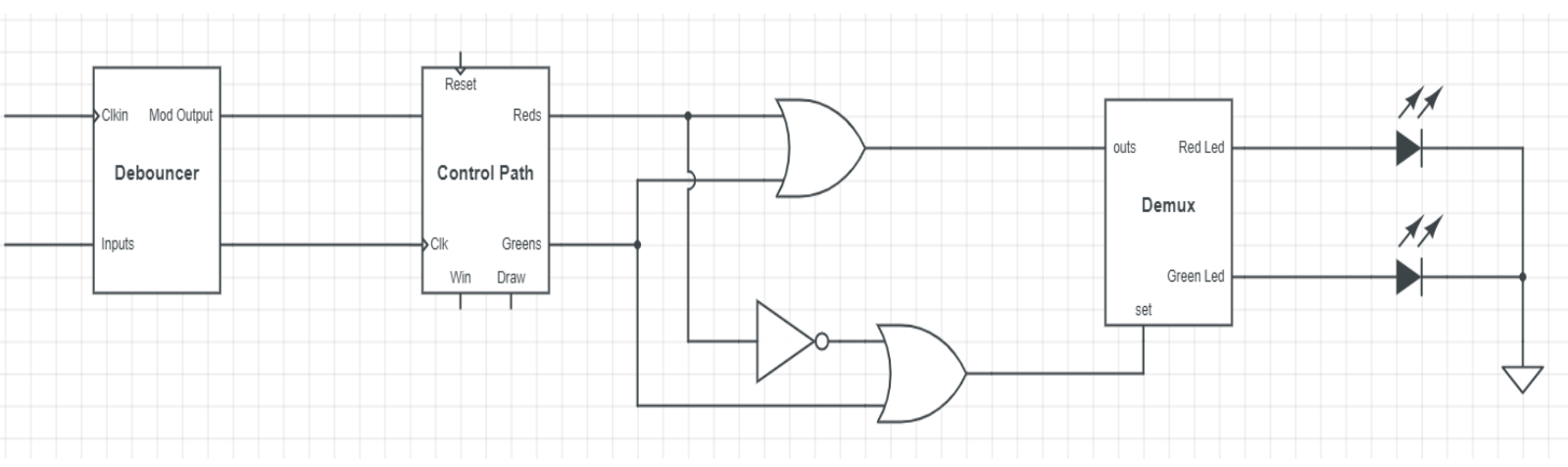
Interconnection of Modules
Debouncing Module
Bouncing is the tendency of any two metal contacts in an electronic device to generate multiple signals as the contacts close or open; debouncing is any kind of hardware device or software that ensures that only a single signal will be acted upon for a single opening or closing of a contact.
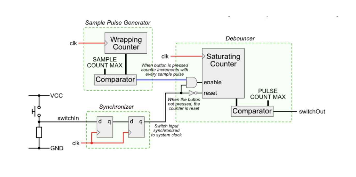
The three main parts are:
-
Sample Pulse Generator - A counter that increments every clock edge. When the maximum is reached a sample pulse is generated and the count value resets to zero. The sample pulse is used to sample the switch input.
-
Synchroniser - The Synchroniser makes sure the switch signal is synchronized with the system clock, the double flip-flop minimizes the chance of metastability.
-
Debouncer - A counter that is incremented every sample pulse whilst the switch is pressed. When the switch is not pressed the counter is reset to zero. If the counter is at its maximum, the debouncer output is high, otherwise, it is low.
Control Path Module
FSM Abstraction
The game starts with player 1 and switches every turn. The win cases are hard-coded and are being checked in each iteration. The draw case is reached if 9 moves are done. The game ends by staying in the finish state until reset.
State Transition
| LABLE | TRANSITION |
|---|---|
| A | Inputs = 0 |
| B | Inputs = 0 |
| C | Reset = 0 |
| D | Win and draw = 0 |
| E | Win and draw = 0 |
| F | Reset = 1 |
| G | Win or Draw = 1 |
| H | Win or Draw = 1 |
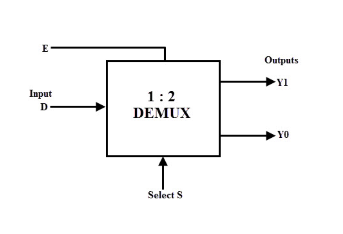
Demux Module
Demultiplexer: De-Multiplexer is a combinational circuit that performs the reverse operation of Multiplexer. It has a single input, n selection lines, and maximum of 2n outputs. The input will be connected to one of these outputs based on the values of selection lines. Since each cell on the led matrix contains two LEDs, the demux is used to determine which LED to turn on.
Procedure
Go through the code to understand the interconnections of different modules and implementing them in the Zybo board.
Implementation
- Follow the breadboard circuit to implement the circuit.
- Take a look at the constraint file to view the mapping of the output and input ports of the Zybo to the circuit.
Win Condition
Draw Condition
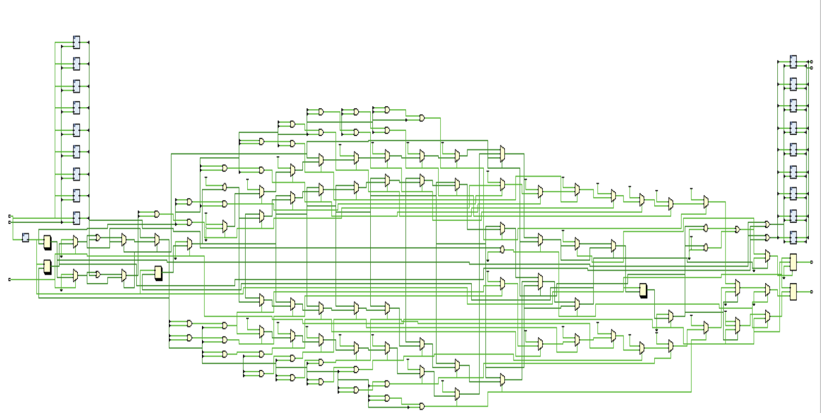
RTL Schematic
In digital circuit design, register-transfer level ( RTL ) is a design abstraction which models a synchronous digital circuit in terms of the flow of digital signals (data) between hardware registers, and the logical operations performed on those signals.
Conclusion
We learned how to code in Verilog effectively and efficiently and also we used some additional syntax taught in class such as genvar etc…, One of the major challenges was debugging the Verilog code. Accepting user input only when he presses input at the right time was the tedious task. Every time we changed a small portion of the code we had to go through the very- long process of running a synthesis, running implementation, and generating bitstream. Only then we were able to debug all the errors. To solve this issue we learned a concept of debouncing which solves this issue and implemented it on Verilog. We also taught to make an illegal handler which prevents the players from giving illegal inputs but we couldn’t implement it as there was some implementation error every time we include that module and we ran out of time. In conclusion, we would like to add by saying that this process of making it was hectic and also fun at the same time. Here is the final project folder TicTacToe Verilog Project. I hope you have fun implementing it!! Don’t lose to your friend :)
References
We didn’t require any additional references or help. We used the concepts learned in the lab over the semester for the implementation of our projects.